
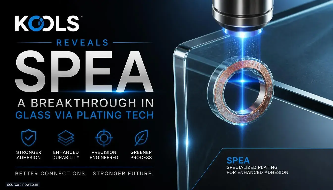
In a move that could reshape semiconductor manufacturing, Kools has unveiled its new SPEA plating technology, engineered specifically for bottom-up glass via filling. This innovation promises to address longstanding challenges in creating more efficient and reliable interconnects in advanced electronics.
Key Facts
- Technology Name: SPEA
- Application: Bottom-up glass via filling
- Developer: Kools
Why This Matters
Glass via filling is a critical step in producing high-density interconnects for semiconductors, and traditional methods often struggle with uniformity and defect rates. SPEA’s bottom-up approach aims to tackle these issues head-on, potentially boosting yield and performance in next-generation devices.
The Technology Behind SPEA
While specific technical details remain under wraps, the bottom-up methodology suggests a focus on precision and control, minimizing voids and improving structural integrity. For an industry constantly pushing the limits of miniaturization, such advancements are not just welcome—they’re essential.
Looking Ahead
As Kools rolls out SPEA, eyes will be on how quickly it’s adopted by major manufacturers. If it delivers on its promises, it could become a new standard in via plating, easing production bottlenecks and supporting the relentless pace of innovation in tech.


Comments